


traditional Energy Financial institution has an excellent slim design")


 with No Value EMI/Extra Trade Gives")
| 2.3 Ghz Octa Core Helio G37| 13 MP AI Triple Digital camera |Fingerprint Sensor| 5000 mAh Battery| Upto 7GB Expandable RAM")
: Take a look at Full Listing of Cheats for this Widespread Sport")
 – Blue")


TSMC introduced its ground-breaking 1.6nm manufacturing course of for chips and it additionally contains bottom energy supply community that improves energy effectivity and transistor density even additional.
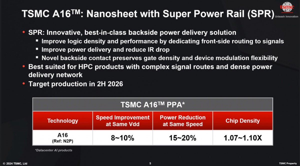
The introduced 1.6nm course of depends on gate-all-around nanosheet transistors, similar to the upcoming N2, N2P and N2X architectures primarily based on the 2nm node. The brand new course of alone permits 10% larger clock speeds on the similar voltage and as much as 20% decrease energy drain on the similar frequency and complexity. Relying on the chip design, the brand new 1.6nm course of may match as much as 10% extra transistors.
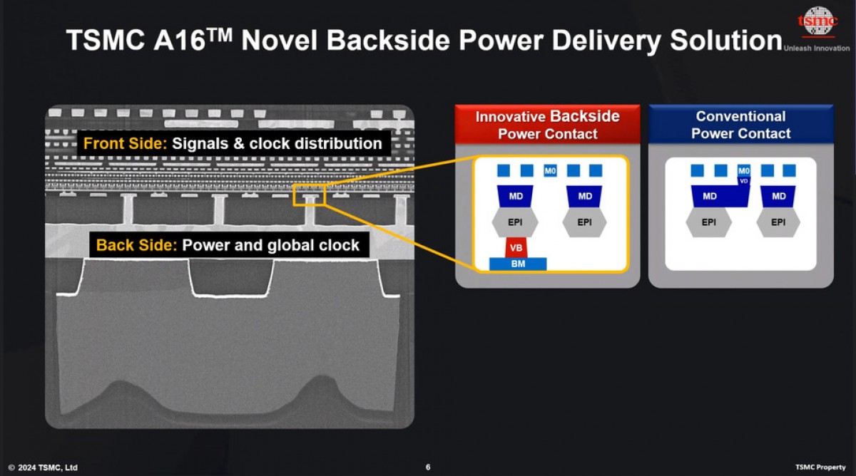
The bottom energy supply community is arguably an much more spectacular facet of those future chips because it allows elevated transistor density and improved energy supply, which in flip impacts efficiency. TSMC says that together with the Tremendous Energy Rail (SPR), which is the kind of plug used to conncect the chip to the ability supply, the bottom energy supply community will show helpful principally to AI and HPC processors that require complicated sign wiring and dense energy networks.
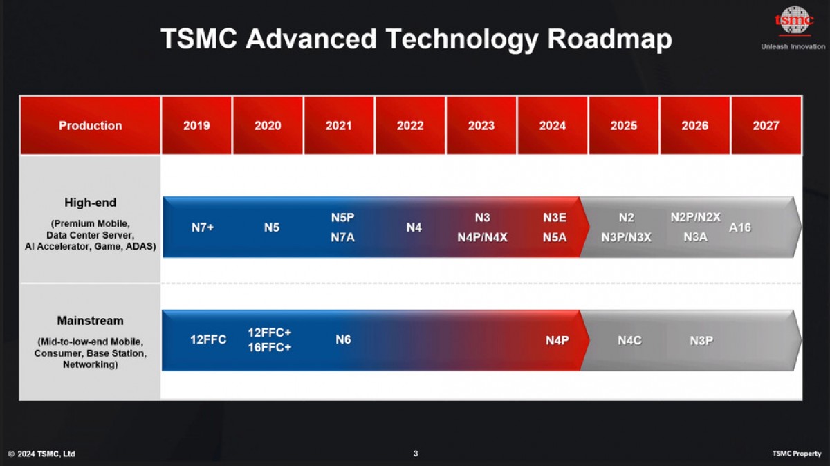
The manufacturing timeline is scheduled for the second half of 2026, if all goes to plan, with the primary consumer-ready merchandise delivery in 2017.